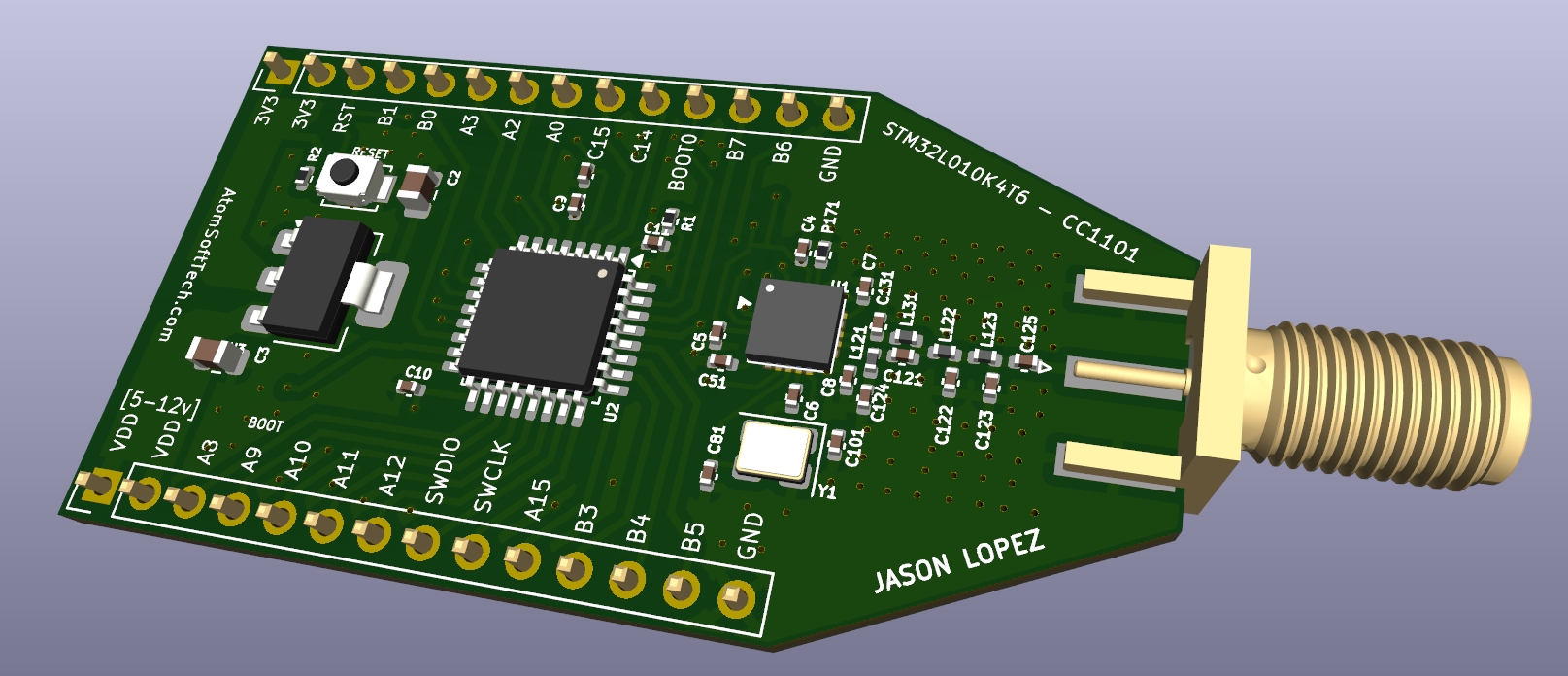
This project is a compact, low-power PCB designed around the STM32L010K4T6 microcontroller paired with the CC1101 Sub-GHz RF transceiver. The goal of this board is to provide a flexible and efficient platform for wireless control, monitoring, or experimentation in the 300–900 MHz ISM bands.
The design prioritizes the 315/433 Bands, low power consumption, and clean RF layout while remaining easy to prototype and expand.
Why STM32L010?
The STM32L010 was selected for several reasons:
- Ultra-low power consumption (ideal for battery-powered devices)
- ARM Cortex-M0+ core with predictable performance
- Adequate flash and RAM for RF protocols and control logic
- Wide operating voltage range
- Strong tooling and ecosystem (STM32Cube, HAL/LL)
Despite its small footprint, the L010 is more than capable of handling packet-based RF communication, timing-sensitive protocols, and peripheral control.
Why CC1101?
The CC1101 is a well-established Sub-GHz transceiver known for:
- Excellent sensitivity and range
- Support for common ISM bands (433 / 868 / 915 MHz)
- Flexible modulation schemes (OOK, FSK, GFSK, MSK)
- SPI interface with good MCU support
- Strong community adoption and documentation
This makes it a great choice for custom RF solutions where off-the-shelf modules are too limiting.
Board Features
- STM32L010K4T6 microcontroller
- CC1101 Sub-GHz RF transceiver
- SPI interface between MCU and RF chip
- External crystal support (RF + MCU if needed)
- Programming/debug header (SWD)
- Decoupling and RF-friendly grounding layout
- Compact form factor suitable for enclosures
Pinout & Signal Mapping
To make development and debugging easier, I mapped all critical signals clearly, including:
- GPIO
- BOOT0 Pin
- SWD programming pins
- Power and ground references

Dimensions:

RF Layout Considerations
Special care was taken with the RF section:
- Short, impedance-aware RF traces
- Dedicated ground stitching around the CC1101
- Proper decoupling near the RF power pins
- Antenna routing kept clean and isolated from digital noise
While this version is still in the prototype stage, the layout follows proven Sub-GHz best practices.
Current Status & Next Steps
- ✅ Schematic complete
- ✅ PCB layout complete
- ✅ 3D render generated
- ⏳ First prototype fabrication (Awaiting OSHPark)
- ⏳ Firmware bring-up and RF testing
Once boards are in hand, I plan to validate RF performance, power consumption, and reliability before iterating further.
Final Thoughts
This project is part of an ongoing effort to build reliable, custom wireless hardware. It’s small, efficient, and intentionally flexible — a solid base for many RF-driven applications.
More updates will follow once the first boards arrive and testing begins.