The below is old news… CHECK OUT SMALLER VERSION
Take a look. Its just PCB design but should be perfectly fine to make 🙂 1.27mm headers
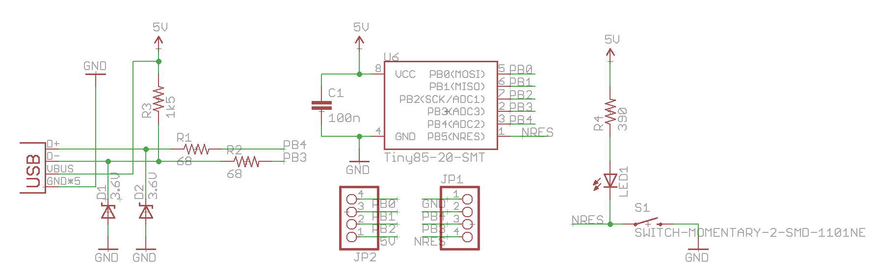
The Image on the left is the main MCU its LEVEL 1 on stack (bottom) (has LED also)
The Middle image is USB and Diodes etc.. its LEVEL 2 on stack (middle)
The Last image on right is the RESET BUTTON its LEVEL 3 on stack (TOP MOST) so its easy to press.
AT MAX ITS 0.24in x 0.41in, If i had a Atiny85 id make these PCBs at home instead of ordering from OSHPark as they are so tiny anyway and have about 3 via max … would be easy to make.
Smallest yet i believe. Schematic below .. EXACT SAME AS ORIGINAL NANITE